
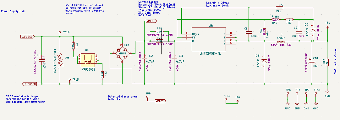
Peak currents in LNK3205 design
I'm designing my first circuit with the LinkSwitch-TN2, in buck and MDCM configuration, for a line-connected AC/DC application. I have read through the data sheet and app notes AN-70 and RDR-721. I've selected the LNK3205 based on maximum current consumption requirements, up to ~ 150mA with everything turned on. I have used the online tool to size the components and spice to model the suggested circuit to estimate maximum currents. I read that you do not offer spice models for your components so I represent the LNK3205 with a pmos switched at constant duty cycle (with 14.3us being the smallest time increment possible with a 70kHz switching frequency), and my load as a resistor. I understand that the result is not accurate, I hope it is nonetheless representative.
Based on the simulation results, I have a few questions :
1. What is the purpose of the LC filter between the output of the rectifier capacitor and the input of the LNK3205 ? The cutoff frequency is pretty high for this application, no ? I understand that the inductor is more efficient than the resistor at higher powers, but why not just add more capacitance ? The current into the LNK is much cleaner with a resistor than with the inductor. Do you recommend for lower noise, a resistor or an inductor ?
1. I have a 230VAC line voltage input and want 6V output. The capacitor-filtered, rectified voltage swings between 320 - 240V. That should result in 1.8-2.5% duty cycle. My simulation shows a duty cycle of 0.3%, set with an on-time of 14.2us (based on 70kHz switching frequency) and 8.5m period. It this a duty cycle reasonable ?
3. At fixed duty cycle my output voltage swings from 5 - 17V. Your design tool says I will get a better result, very good. However, I get a peak current of 3.5 - 5A out of L2 (output inductor), depending on its inductance, following the brief on-time. This seems really high. Can you confirm that the output current will be in this order of magnitude for my implementation ?
Thanks in advance for your clarifications. The LNK3205 seems like a great component, I'm looking forward to getting to understand it better.
Files
| Attachment | Size |
|---|---|
| Simulation Model | 66.55 KB |
| Schematic | 69.03 KB |
Hi Greanie!
Thanks for looking into using LNK-TN2. I hope that it will be suitable for your needs.
PI-CookieMonster